Scanning Electron Microscopy (SEM)
There are two scanning electron microscopes at the Center for Advanced Microscopy, an ultra-high resolution JEOL 7500F with a cold field emission emitter and a JEOL 6610LV with a tungsten emitter. Both are equipped with Oxford EDS systems for elemental analysis.
The 6610LV SEM offers excellent SEM imaging in the range of 5X to 30,000X and is our 'workhorse' instrument.

Electron gun
- W filament
Vacuum modes
- Conventional high vacuum
- low vacuum (up to 270 Pascals) for un-coated / non-conductive or volatile samples
Available detectors
- Secondary electron (SEI, Everhart-Thornley)
- Backscattered electron (BEI).
- Three active segments allow discrimination of compositional, topographic, or stereographic 'shadow' signals
- Low-vacuum secondary electron detector (LSED)
X-ray analysis
- Oxford X-Max 20 mm2 SDD
- Point analysis, line scan, and mapping capabilities
Stage rotation and tilt
- 'Five-axis' stage capable of x, y, z translation, rotation, and tilt
- Tilt -10 to 90 degrees, depending on sample holder used, specimen size/shape, and working distance
Sample holders and specimen sizes
The large sample chamber accepts samples up to 200 mm wide and 80 mm thick, with several types of sample 'pucks' for different sizes and shapes. See our 'how to prepare samples' page for more details.
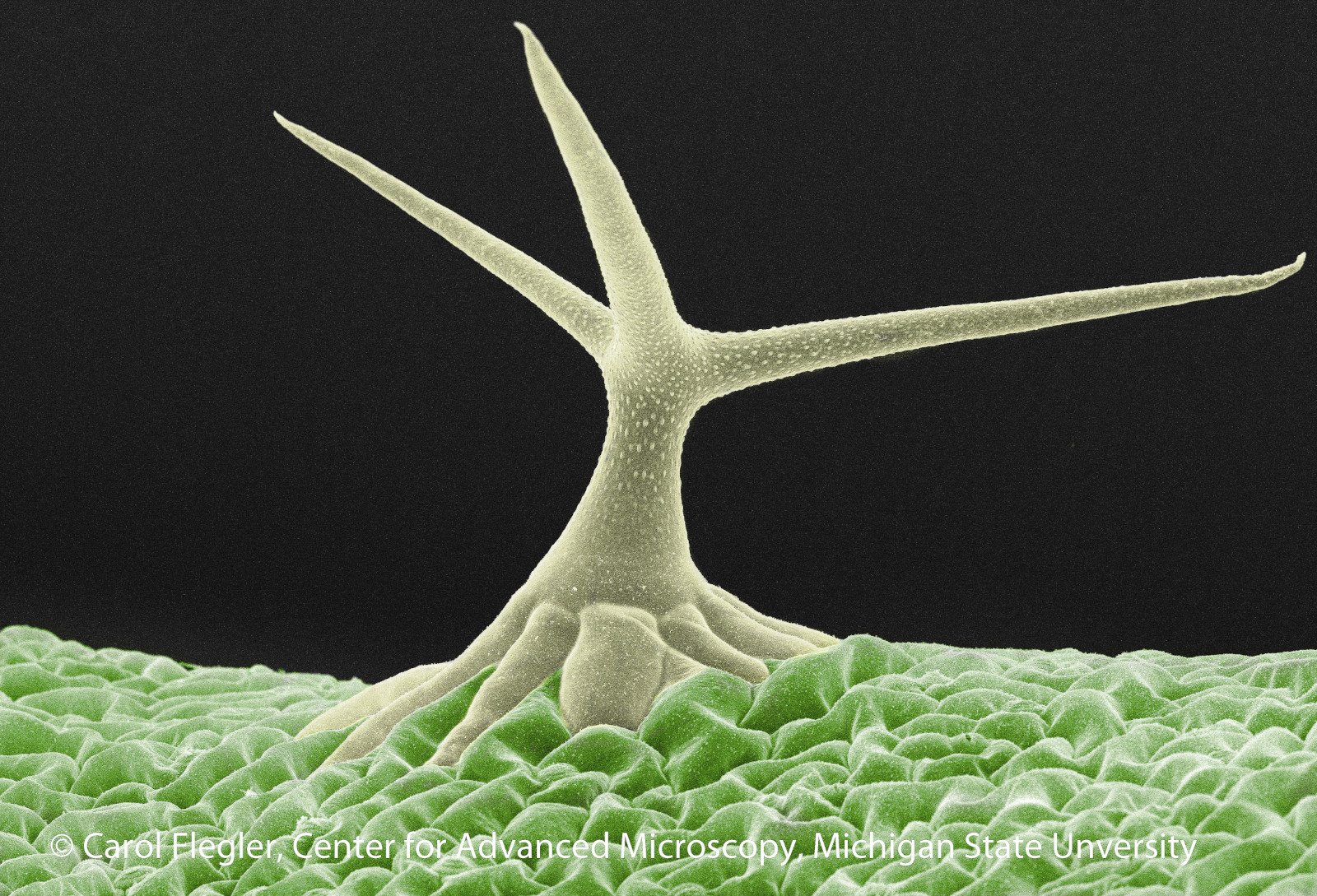
Trichome on the leaf of the plant Arabidopsis thaliana, a plant used as a model organism for scientific experiments. This image was taken on the JEOL 6610LV scanning electron microscope at the Center for Advanced Microscopy. All SEM images are black and white; color was added using software.
The 7500F SEM is designed for the most demanding applications in the range of 1,000X to 1,000,000X. It is the highest resolution SEM in the State of Michigan. The 7500F is designed for maximum resolution and information extraction by use of multiple advanced secondary and backscattered electron detectors, a special energy filter for the detected electrons, and electron beam deceleration. It has outstanding resolution at a 1 kV accelerating voltage where many non-conductive samples can be examined without a conductive coating.

The JEOL 7500F ultra-high resolution scanning electron microscope at the Michigan State University Center for Advanced Microscopy
Electron gun
- Cold field-emitter
Vacuum modes
- Conventional high vacuum only
Available detectors
- Upper Secondary Electron (SEI, in-lens)
- Lower Secondary Electron (LEI, Everhart-Thornley)
- Retractable In-lens Backscattered Electron (RIBE), very high-resolution imaging at low working distance; can be used with Gentle Beam mode
- Low-Angle Backscattered Electron (LABE), high-resolution low-kV imaging at analytical working distance
- Transmission Electron Detector (TED), detects transmitted electrons and can be used with Transmission Electron Microscopy grids
Imaging aides
- Aperature angle control lens (ACL): can be set for
- maximum resolution (smallest spot size) or
- increased depth of field
- Gentle beam mode: beam deceleration
- GB-L 'low', reduce sample charging
- GB-H 'high', higher mag low kV imaging (no tilting)
- r-filter: used to select energy range of electrons reaching the SEI in-lens detector.
Can be used for
- emphasizing topographic or Z-contrast
- excluding electrons that contribute to sample charging
X-ray analysis
- Oxford X-MaxN 150 mm2 SDD
- Point analysis, line scan, and mapping capabilities
Stage rotation and tilt
- 'Five-axis' stage capable of x, y, z translation, rotation, and tilt
- Tilt -5 to 60 degrees, heavily dependent on sample holder used, specimen size/shape, and working distance
Sample holders and specimen sizes
The largest samples that can be accomodated are a maximum of approximately 2" x 1.75", depending on the height and sample geometry. See our 'how to prepare samples' page for more details.
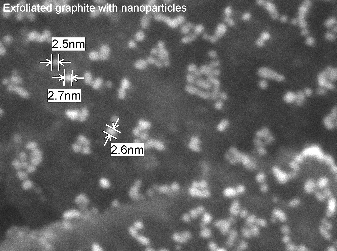
Exfoliated graphite with nano-particles. Image taken at a magnification of 1,000,000X on the JEOL 7500F scanning electron microscope. Research from the lab of Lawrence Drzal.
Coating and sample preparation capabilities:
- Gold sputter coating
- Iridium coating
- Platinum coating
- Osmium coating for ultra-high resolution
- Carbon coating
Critical point drying
Freeze drying
See our Sample preparation equipment page for more details on the equipment, and our 'how to prepare samples' page for more details on sample preparation procedures.
 For SEM services contact either Amy Albin, albinamy@msu.edu, or Abby Vanderberg, vandera@msu.edu.
For enrollment in the SEM Lab course, contact Andy Elwood Madden (maddenan@msu.edu). This is a limited enrollment course with specific enrollment procedures. Please see our Courses page for more information.